Vogel Homebrew · Volume 3
Vogel homebrew analog computer — Volume 3 — The linear computing elements
Summers, integrators, the open amplifier and the coefficient potentiometers, walked with the schematic open — and the integrator input networks that do not come to the round numbers the panel implies
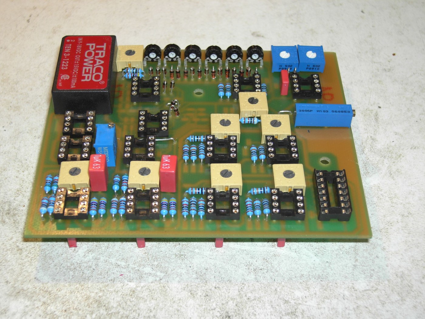
Figure 1 — The main board, component side, of a machine built to this design. Every computing element in this volume is on this board: the DIP sockets in the lower two rows take the LF355 amplifiers, the white multi-turn trimmers are the per-amplifier offset adjustments P1–P6, and the two red capacitors are the integrating capacitors C1 and C2. Photograph: attributed to Bernd Ulmann / analogmuseum.org, March 2010.
3.1 About this Volume
This volume walks the machine’s linear computing elements with the schematic sheet open: the three summers, the two integrators and their mode switch, the open amplifier, and the four coefficient potentiometers. Every designator and value given here is transcribed from that sheet. Where something is analysed rather than transcribed — and two of the more interesting passages are analysis — the text says so in the sentence that does it.
Cross-references: Vol 1 for the sources and the specification tables; Vol 2 for the panel terminals these circuits appear on; Vol 4 for the multiplier and the sine generator; Vol 5 for the reference supply that every coefficient is a fraction of; Vol 6 for the programs.
3.2 The Common Amplifier
Six of the machine’s twelve integrated circuits are the computing amplifiers, and all six are the same part: an LF355, one amplifier per package, in the six positions IC1 to IC6.
Table 1 — The Common Amplifier
| Designator | Element | Panel column |
|---|---|---|
| IC1 | Integrator 1 | INT1 |
| IC2 | Integrator 2 | INT2 |
| IC3 | Summer 1 | SUM1 |
| IC4 | Summer 2 | SUM2 |
| IC5 | Summer 3 | SUM3 |
| IC6 | Open amplifier / inverter | OP/I |
The LF355 belongs to the LFx5x family — JFET-input, bipolar-output monolithic amplifiers in what the manufacturer called BI-FET technology. The 2009 description gives the properties it was chosen for: input resistance 10¹² Ω, open-loop gain greater than 3 × 10⁵, offset voltage typically 5 mV.
The first of those three is the one that matters most for this machine, and it is worth being explicit about why. In an analog computer the integrator is the element that fails first and fails quietly: any current that enters the summing junction from somewhere other than the input network charges the integrating capacitor, and the machine has no way to tell that current apart from a real input. A JFET-input amplifier reduces that parasitic current by three or four orders of magnitude relative to a bipolar-input part. Section 4 below turns the machine’s own published droop figure into a number and shows that it lands exactly where the amplifier’s bias current puts it.
Note — The datasheet held alongside these documents (Texas Instruments LFx5x JFET Input Operational Amplifiers, SNOSBH0D) lists on its front page a typical large-signal DC voltage gain of 106 dB, which is about 2 × 10⁵, against the 2009 description’s ”> 3 × 10⁵”. Both are of the same order and the difference makes no practical difference at these closed-loop gains, but the two figures are not the same figure and neither source is adjusted here to match the other.
3.2.1 Offset Trimming and Decoupling
Every one of the six amplifiers carries its own offset trimmer — P1 to P6, 50 kΩ each — connected across the device’s two offset-null pins with the wiper returned to +15 V. That arrangement is the manufacturer’s own recommended null circuit for this family, and the family’s datasheet makes a point of it: offset adjustment on these parts “does not degrade drift or common-mode rejection”, which is not true of most monolithic amplifiers and is the reason a per-amplifier trimmer is worth six components.
Every amplifier also carries a 0.1 µF decoupling capacitor on each rail — C3/C4 for IC1, C5/C6 for IC2, and so on to C13/C14 for IC6. Twelve capacitors for six amplifiers, with no shared bulk decoupling drawn on the computing side of the sheet. On a board 105 × 88 mm carrying both the computing elements and a switching DC/DC converter, that is not belt-and-braces; Vol 5 §3 treats the converter’s switching noise as the design constraint it is.
3.3 The Summers
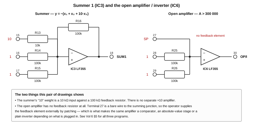
Figure 2 — Summer 1 (IC3) and the open amplifier (IC6), redrawn from the schematic sheet. Diagram authored for this dive.
All three summers are identical. Taking Summer 1 as drawn:
Table 2 — All three summers are identical. Taking Summer 1 as drawn
| Designator | Value | Terminal | Role |
|---|---|---|---|
| R13 | 10 kΩ | 15 | weight-10 input |
| R14 | 100 kΩ | 16 | weight-1 input |
| R15 | 100 kΩ | 17 | weight-1 input |
| R16 | 100 kΩ | — | feedback |
| P3 | 50 kΩ | — | offset null |
| — | — | 18 | output |
Summers 2 and 3 repeat the pattern exactly: R17–R20 with P4 and terminals 19–22, and R21–R24 with P5 and terminals 23–26.
The transfer function follows immediately from the resistor ratios and is stated in the description as
y = −(x₁ + x₂ + 10·x₃)
with a stated achievable static computing error of ≤ 0.1 %.
Three observations about this arrangement are worth making, because they are design decisions rather than consequences.
There is no ×10 amplifier. The gain of ten is a property of one input of each summer, not of a separate element. A program that needs a variable multiplied by ten spends a summer input on it, and gets a sign inversion it did not ask for as part of the bargain. This is why the workbook’s programs are full of inverters: on a machine with three summers and one open amplifier, sign management is a real resource constraint, and Vol 6 §2 shows how the published programs manage it.
The feedback resistor is on the board, not on the panel. Unlike the EC-1, where the operator plugs the feedback element into a socket and thereby decides what each amplifier is, here a summer is permanently a summer. The gain structure of the machine is fixed in copper. That is what a demonstrator sized to a known problem set can afford, and it is also what makes the machine impossible to repurpose.
100 kΩ is the machine’s working impedance level. Every summer input and every summer feedback resistor is 100 kΩ or a decade below it. That choice sets the amplifier’s noise gain, the loading it presents to whatever drives it, and — critically — the loading that a 10 kΩ coefficient potentiometer presents into it, which §6 below computes.
3.4 The Integrators
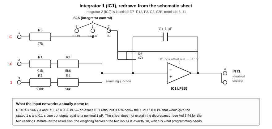
Figure 3 — Integrator 1 (IC1), redrawn from the schematic sheet. Diagram authored for this dive.
Both integrators are identical. Taking Integrator 1 as drawn:
Table 3 — Both integrators are identical. Taking Integrator 1 as drawn
| Designator | Value | Terminal | Role |
|---|---|---|---|
| R5 | 47 kΩ | 1 | initial-condition input |
| R6 | 47 kΩ | — | initial-condition feedback path, switched |
| R1 + R2 | 91 kΩ + 5.6 kΩ | 2 | weight-10 input network |
| R3 + R4 | 910 kΩ + 56 kΩ | 3 | weight-1 input network |
| C1 | 1 µF | — | integrating capacitor |
| S2A | 3-position | 5, 6, 7 | RUN / HOLD / IC |
| P1 | 50 kΩ | — | offset null |
| — | — | 4 | output (doubled socket) |
Integrator 2 repeats it: R11 and R12 at 47 kΩ, R7 + R8 at 91 kΩ + 5.6 kΩ, R9 + R10 at 910 kΩ + 56 kΩ, C2 at 1 µF, switch section S2B on terminals 12–14, offset trimmer P2, output on terminal 11.
3.4.1 The Three Modes
The description gives the behaviour of the three switch positions directly:
Table 4 — The description gives the behaviour of the three switch positions directly
| Position | Behaviour | Transfer function |
|---|---|---|
| IC | ”the inverted voltages of the IC inputs are present at the integrator outputs” | y = −IC |
| RUN | ”the input signals are integrated” | y = −∫₀ᵗ(x₁ + 10·x₂)dt − IC |
| HOLD | ”the integration process is paused and the last achieved output voltages are saved” | y = constant |
The equality of R5 and R6 at 47 kΩ is the mechanism behind the IC mode, and it is worth spelling out because it is elegant and because nothing in the description explains it. A unity-gain inverter is an amplifier with equal input and feedback resistors. In the IC position the switch places R6 in the feedback path alongside the capacitor and connects the IC input network, and the amplifier becomes exactly that: a unity inverter from terminal 1, giving y = −IC and simultaneously charging C1 to that same voltage. The initial condition is not injected into the capacitor by a separate charging circuit, as on the EC-1; the integrator is temporarily turned into an inverter and the capacitor ends up where it needs to be as a side effect. Switching to RUN removes R6, restores the input network, and integration begins from exactly the voltage the amplifier was already holding — with no transient, because nothing about the amplifier’s output had to change.
The sheet supports the reading directly: R6 is drawn between the switch and the amplifier’s output node, in parallel with C1. When the switch connects it, the integrator has a resistor across its capacitor and becomes a finite-gain inverting stage; when the switch opens it, the capacitor is alone in the feedback path and the element integrates.
Note — The switch contacts are themselves numbered terminals — 5, 6 and 7 for S2A, 12, 13 and 14 for S2B — and are drawn on the sheet as patching sockets like any other. Whether all three are actually brought out to the panel could not be determined: the panel artwork shows no sockets in those positions, and the 2009 description mentions none. The most likely reading is that the numbering scheme covers every terminal on the board, panel-facing or not.
Both integrators are driven by one switch, and there is no per-integrator mode control. This is a consequential simplification: a second-order program has both integrators in the same loop and must start them simultaneously, which one switch guarantees and two switches would not.
3.4.2 The Droop Figure, and What It Confirms
The description gives one number for HOLD performance: the outputs fall by “approximately 6 mV per minute” through discharge of the integrating capacitors.
That figure is checkable, and checking it is the cleanest confirmation available that the machine is what it says it is. The current that produces a given rate of change on a capacitor is
I = C · dV/dt = 1 µF × (6 mV / 60 s) = 1 × 10⁻⁶ × 1 × 10⁻⁴ = **100 pA**One hundred picoamps of total leakage at the summing junction — the amplifier’s input bias current, plus the capacitor’s own leakage, plus whatever the board’s surface contributes. The LFx5x datasheet’s front page gives a typical input bias current of 30 pA. The published droop is therefore consistent with an amplifier of this family working into a capacitor of ordinary quality on a board of ordinary cleanliness, with the amplifier contributing roughly a third of it.
Note — The arithmetic above is analysis performed for this series, not a figure quoted from any held source. Its value is as a consistency check: had the published droop implied a leakage of, say, 100 nA, it would have meant the machine did not have JFET-input amplifiers at its integrators, and the description’s claim would have needed re-examining. It does not.
The practical reading for an operator is that HOLD is genuinely usable. Six millivolts is 0.0006 machine units. A problem can be held for a minute while the address selector is walked around every element and each output written down, and the error introduced by the holding is two orders of magnitude below the summers’ own 0.1 %.
3.5 The Integrator Time-Constant Question
The description states the integrator time constants without ambiguity: 1 second on the weight-1 input, 0.1 second on the weight-10 input, with a tolerance of ±1 %. The panel labels agree. The programs in the workbook are computed on that basis and say so — “T = 1 s was chosen as the time constant for the integrator.”
The schematic does not give those values.
Table 5 — The Integrator Time-Constant Question
| Input | Resistors as drawn | Series total | × 1 µF |
|---|---|---|---|
| weight-1 | R3 910 kΩ + R4 56 kΩ | 966 kΩ | 0.966 s |
| weight-10 | R1 91 kΩ + R2 5.6 kΩ | 96.6 kΩ | 0.0966 s |
Both networks are 3.4 % below the 1 MΩ and 100 kΩ that would produce the stated constants against a nominal 1 µF — more than three times the ±1 % tolerance the description claims for them.
The values are plainly deliberate. A designer wanting 1 MΩ from this parts bin would fit a 1 MΩ resistor, or 910 kΩ + 91 kΩ. Choosing 910 kΩ + 56 kΩ is a decision to land on 966 kΩ specifically, and the second network repeats it exactly one decade down. Two readings account for that, and the held sources do not decide between them.
Reading A — the resistors compensate a known capacitor. The description’s ±1 % tolerance is quoted on the time constant, not on the capacitor. The resistors are selected parts; the capacitors are not described at all. If the integrating capacitors were measured at about 1.035 µF, then 966 kΩ × 1.035 µF = 1.000 s exactly, and every stated figure is correct. On this reading the odd resistor values are the trim, and the machine has no adjustable integrator calibration because it does not need one.
Reading B — the time constants really are 0.966 s. The description’s “1 s” and “0.1 s” are then nominal statements of intent, and the ±1 % claim applies to the matching between units rather than to the absolute value.
Reading A is the more economical, because it explains the resistor choice and Reading B does not; it is nonetheless inference, and it is labelled as such here. A reader with the machine on a bench can settle it in five minutes with a capacitance meter.
Two things are certain regardless of which reading is right, and both matter more than the question itself:
The ratio between the two inputs is exactly ten. 966 ÷ 96.6 = 10.000, to as many figures as the resistors hold. Every program in the workbook that mixes weight-1 and weight-10 inputs depends on that ratio and not on the absolute constant, and the ratio is exact by construction.
Any absolute error is common to both integrators, since they are built from the same four values. A second-order program’s frequency would shift by 3.4 % under Reading B, but its damping ratio and its shape would not, because both depend on ratios of integrator gains. The most visible consequence of Reading B being correct would be that the undamped oscillator of workbook §7.2, computed at 0.159 Hz, would actually run at 0.165 Hz — a difference of one part in thirty, invisible on an oscillogram recorded at one second per division.
3.6 The Open Amplifier
The sixth amplifier, IC6, is the one element in the machine whose function is not fixed. Its circuit is the shortest on the sheet:
Table 6 — The sixth amplifier, IC6, is the one element in the machine whose function is not fixed. Its circuit is the shortest on the sheet
| Designator | Value | Terminal | Role |
|---|---|---|---|
| R25 | 100 kΩ | 28 | weight-1 input |
| R26 | 100 kΩ | 29 | weight-1 input |
| — | — | 27 | summing point, brought out bare |
| P6 | 50 kΩ | — | offset null |
| — | — | 30 | output |
There is no feedback resistor. The amplifier runs open-loop, at the full gain of the device — the description gives ”> 300 000” — and its output is therefore at one saturation rail or the other for any input difference above a few tens of microvolts. The workbook gives the saturation figures as approximately ±14 V, which is what an LF355 on ±15 V rails does.
That makes the element three different things depending on what the operator patches:
Table 7 — That makes the element three different things depending on what the operator patches
| Patch | Behaviour | Used in |
|---|---|---|
| Output wired back to input 29 (terminal 30 → 29) | unity inverter, y = −x₁ | everywhere; the machine’s only spare inverter |
| Nothing in feedback; two variables on 28 and 29 | comparator — output slams to ±14 V on the sign of the difference | Vol 6 §5.1 |
| Diode cable in the feedback path via terminal 27 | precision rectifier / absolute-value element | Vol 6 §5.3 |
| Any external element between 30 and 27 | whatever that element makes it | — |
Terminal 27 is what makes the last two possible, and its importance is easy to under-read. It is a bare wire to the summing junction — no resistor, no protection, no buffering. Patching a component between terminals 30 and 27 places that component in the amplifier’s feedback path, which is precisely the EC-1’s plug-in feedback socket recreated with two patch cords. On a machine whose other five amplifiers have their feedback soldered down, this one terminal carries the entire capacity for non-linear and discontinuous programming.
Warning — Terminal 27 is a summing junction at a virtual ground, fed by nothing. A patch cord from any signal output directly to terminal 27, with no series element, drives the amplifier’s input from a low-impedance source through no resistance at all; the amplifier saturates immediately and the driving element sees a short to virtual ground. The workbook’s discontinuous-function programs always place a diode or a resistor in that path. The description does not warn about this and the panel does not mark it.
Note — As set out in Vol 1 §7 and Vol 2 §4, the schematic sheet mislabels terminal 27 with the weight glyph “10”. The panel artwork and §3.3 of the description both call it the summing point, and the circuit — a bare wire — admits no weight at all.
3.7 The Coefficient Potentiometers
Four ten-turn potentiometers with lockable dials, P21 to P24, 10 kΩ each, giving y = k·x for 0 ≤ k ≤ 1. K1 and K2 have their lower ends grounded. K3 and K4 have their lower ends taken to switch S5 and to a panel socket, as Vol 2 §5 describes.
Setting a coefficient is described in one sentence: “For precise adjustment of the coefficients, the reference voltage +10.00 V and an external digital voltmeter are used.” The operator patches the +1 reference into the pot, selects that pot on the address selector, and turns the dial until the DVM reads ten times the wanted coefficient.
That procedure looks like a convenience. It is in fact the machine’s answer to a real problem, and the arithmetic is worth doing.
A 10 kΩ potentiometer feeding a 100 kΩ summer input is not a lightly loaded divider. With the wiper at mid-travel the pot’s lower half — 5 kΩ — is in parallel with the 100 kΩ input resistor returning to a virtual ground, giving 4.76 kΩ against an upper half of 5 kΩ. The delivered coefficient is then 4.76 / (5 + 4.76) = 0.488, not 0.500. The error is about 2.4 % of full scale at mid-setting, falling to zero at both ends of travel — and it is more than twenty times the summers’ own computing error.
Note — The loading arithmetic above is analysis performed for this series. Neither the description nor the workbook mentions potentiometer loading.
Two features of the machine make that error disappear rather than merely tolerable:
The coefficient is set in circuit, against the delivered voltage. Because the address selector taps the potentiometer output — not the dial, not the top of the track — the DVM reads the voltage the summer will actually receive, with the loading already in it. Turning the dial until the DVM says what it should say sets the effective coefficient correctly whatever the load is. The dial position is then not 0.500 and the lockable scale will not read 0.500; the coefficient nonetheless is.
This is why the address selector has coefficient-potentiometer positions at all. Four of its twelve positions monitor things that are not computing elements and produce no answers. They exist so that coefficients can be set the way described. Vol 5 §6 returns to this.
The corollary for an operator is a discipline, and it is the single most important operating habit on this machine: set every coefficient after the program is patched, never before. A potentiometer set against an open circuit and then wired into a summer will deliver a coefficient up to 2.4 % below its dial — and the error will be largest exactly at the mid-range settings that most programs use.
3.8 The Linear Error Budget
Collecting what the sources state and what the sections above derive:
Table 8 — Collecting what the sources state and what the sections above derive
| Contribution | Magnitude | Basis |
|---|---|---|
| Summer static computing error | ≤ 0.1 % | stated, 2009 description §3.1 |
| Resistor selection | ±0.05 % on accuracy-relevant parts | stated, §1 |
| Integrator time-constant tolerance | ±1 % | stated, §1 |
| Integrator absolute constant | possibly 3.4 % low | §4 above; unresolved |
| Integrator droop in HOLD | 6 mV/min = 0.0006 MU/min | stated, §3.2 |
| Amplifier offset, untrimmed | 5 mV typical = 0.0005 MU | stated, §1 |
| Coefficient potentiometer loading | up to 2.4 % if set out of circuit | analysis, §6 above |
| Coefficient potentiometer loading | nil if set in circuit | analysis, §6 above |
| Meter reading | class 2.5 — not a computing error | stated, §3.8; see Vol 5 §5 |
The shape of that table is the honest summary of the machine’s linear accuracy. The computing elements are good to a tenth of a percent; the ways of getting numbers into and out of them are between ten and a thousand times worse. Setting coefficients in circuit against a DVM closes the input side of that gap. Reading answers on an external DVM rather than the panel meter closes the output side. Doing neither leaves a machine that computes to 0.1 % and is used to 2 %.
3.9 What Comes Next
Vol 4 takes the two non-linear elements: the AD534K multiplier unit with its four patched functions, and the eleven-segment sine generator breakpoint by breakpoint. Vol 5 covers the reference supply that every coefficient in this volume is a fraction of, along with the supply, metering and monitoring circuits. Vol 6 puts the elements described here to work on the twenty published programs.
Comments (0)