EAI PACE TR-10 · Volume 3
EAI PACE TR-10 — Volume 3 — The computing components
Every module EAI catalogued for the machine, by type number, with its specified performance, its patch-panel face and its place in the row
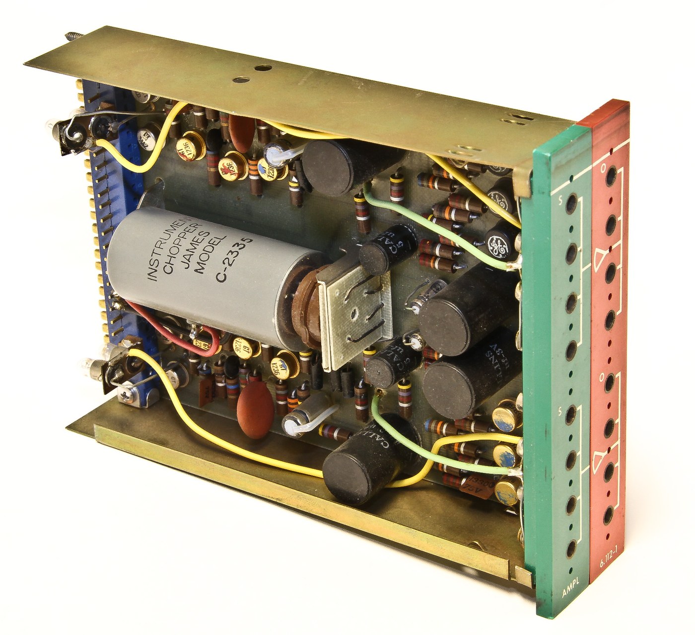
Figure 1 — A TR-10 computing component out of the console. The patch-panel face — the coloured strip at the right — is the module’s front; everything behind it is the computing circuit. This is the unit of capability on the TR-10: the machine is whatever collection of these happens to be plugged in. Photograph: locally held collector image.
3.1 About this Volume
This volume is the catalogue. It lists every computing component and accessory EAI named for the TR-10 in the sixteen-page brochure, with the type numbers, the specified performance figures from GPAC-TR-10 PS 6305 where the specification covers them, and the patch-panel dimensions and colour of each face.
Two limits should be stated before the catalogue begins. First, no schematic for any TR-10 module is held in this project’s library (Vol 1 §3). What follows describes what each module does and what it is specified to achieve; it cannot describe how the circuit inside achieves it. Second, where the brochure and the specification give different figures, both appear and the divergence is marked — Vol 6 collects them.
Cross-references: Vol 2 for the console areas and position rules; Vol 4 for how these modules are combined into a program; Vol 5 for the integrator networks in repetitive operation.
3.2 Reading a Module
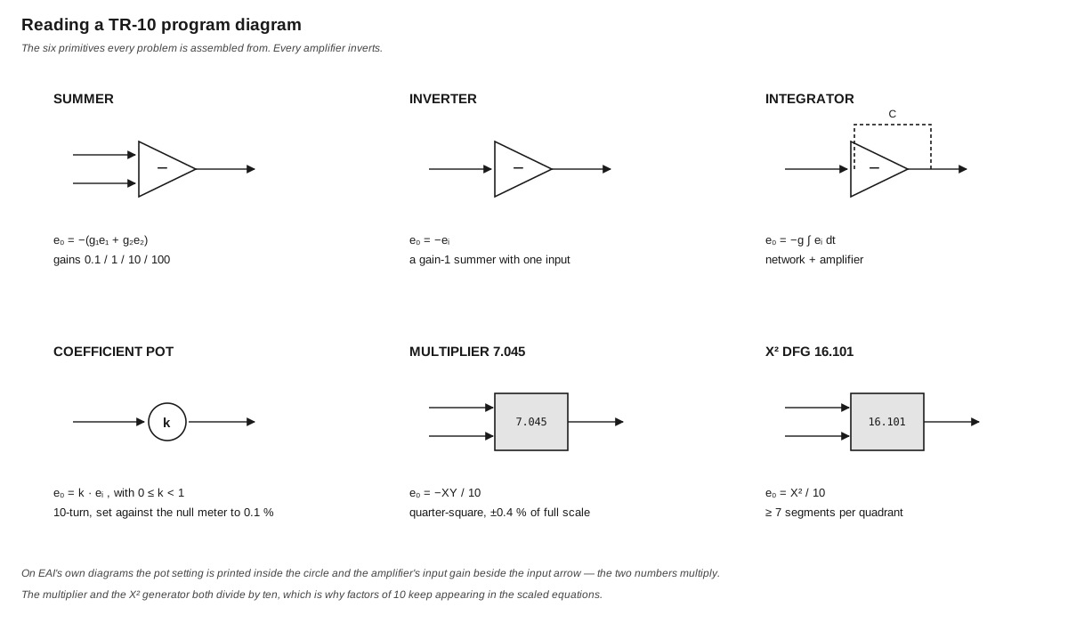
Figure 2 — The computing primitives and their transfer functions. Diagram authored for this dive.
3.2.1 The Physical Format
Every module shares a common face height and one of two widths.
Table 1 — 2.1 The Physical Format
| Property | Value |
|---|---|
| Patch panel height | 5 inches, universally |
| Patch panel width | 1½ inches (full width) or ¾ inch (half width) |
| Retention | two nuts at the rear of the console |
| Insertion | from the front |
Full-width modules occupy two adjacent odd-and-even positions in the non-linear row; half-width modules occupy one. The colour of the face encodes the function of its terminations (Vol 2 §4.2).
3.2.2 Type Numbers
EAI’s type numbers take the form n.nnn and are not sequential by function — 6.282 is an amplifier, 6.143 a comparator. They appear silkscreened on the module face itself, which makes them the most reliable identification on a surviving machine. Where this volume gives two numbers for one thing, that is because the brochure does; see §3.2 and §6.1.
3.3 Operational Amplifiers
3.3.1 Dual Operational Amplifier, Type 6.282
The amplifier is the machine’s active computing element. Everything else either feeds it, scales it, or switches it.
Table 2 — 3.1 Dual Operational Amplifier, Type 6.282
| Property | Value | Source |
|---|---|---|
| Amplifiers per module | 2 | brochure |
| Maximum in console | 20 (10 modules) | brochure, spec §1.3 |
| Stabilisation | individually chopper-stabilised | brochure |
| Construction | fully transistorised | brochure |
| Inputs | single-ended | brochure |
| Output | ±10 V at 20 mA | spec §3.3 |
| Bandwidth | 200 kc minimum | spec §3.4 |
| Offset at summing junction after balance | ≤ 20 µV | spec §3.6 |
| Drift, gain-one integrator | ≤ 50 µV/s | spec §3.7 |
| Phase shift, standard inverter, 20 V p-p at 1 kc | ≤ 0.1° | spec §3.5 |
| Dynamic amplitude error, standard inverter, 10 V p-p at 1 kc | 0.06 % typical, 0.1 % maximum | spec §3.9 |
| Patch panel | 5 in × 1½ in; green (inputs), red (outputs) | brochure |
Three properties deserve comment.
Uncommitted. Specification §3.1 is emphatic: “All operational amplifiers shall be uncommitted. That is, shall be capable of being used as either integrators, summers, or high-gain amplifiers, depending upon the patching utilized.” No amplifier is dedicated to a role by the hardware. An amplifier becomes an integrator only because an integrator network has been patched across it with two patch cords, and it stops being one when they are pulled.
Summing junctions are brought out. The brochure: “Summing junctions of all amplifiers are available at the patch panel so that any amplifier may be used for a variety of mathematical operations.” This is what makes the machine general. The summing junction is the node at which currents from input resistors add; exposing it means the operator, not the designer, decides what feedback element and what inputs an amplifier has.
Balance is remote. “Simple remote adjustments are provided to facilitate manual balancing of amplifiers.” Combined with the panel’s stabilizer-output selection (Vol 2 §6.4), an amplifier can be balanced from the operator’s chair rather than at the module.
Note — The 20 µV offset figure is worth holding against the ±10 V signal range. Twenty microvolts on ten volts is two parts per million, which is far finer than anything else in the machine — the potentiometers resolve to 0.025 %, the multipliers to 0.4 %. The amplifier is deliberately not the limiting element.
3.4 Integrator Networks
3.4.1 What the Network Is
The integrator network is not an amplifier. It is the package of feedback capacitors and mode relays that converts an amplifier into an integrator. This separation is the reason the amplifiers can be uncommitted.
Table 3 — 4.1 What the Network Is
| Property | Value | Source |
|---|---|---|
| Networks per module | 2 (dual) | brochure |
| Maximum in console | 9 dual networks, positions #1–#18 | brochure p. 12 |
| Capacitors | 10 µF, ±0.1 %, polystyrene, used throughout | brochure |
| Capacitor tolerance required | ±0.1 % | spec §3.8 |
| Patching to an amplifier | two patch cords | brochure |
| Initial condition | introduced from any potentiometer into the “IC” termination | brochure |
| Patch panel | 5 in × 1½ in; white | brochure |
The brochure’s description of the mode relays is the key architectural fact: “Contains all relays necessary for switching the computer to various modes of operation; i.e., IC (Initial Condition), Hold, Operate. Relay operation is controlled by computer mode switch on control panel.”
The relays are therefore distributed into the networks, one set per integrator, and the panel’s mode buttons merely energise them. Vol 5 shows why this placement is what makes individual mode control possible as a later modification, and the German dealer newsletter’s field change is exactly an exploitation of it.
Every integrator can be given a non-zero initial condition: “All integrators may thus receive non-zero initial conditions, if required.” On a machine solving a second-order equation this is not a luxury — the two initial conditions of the problem are precisely two integrator IC voltages, as Vol 4 §5 demonstrates.
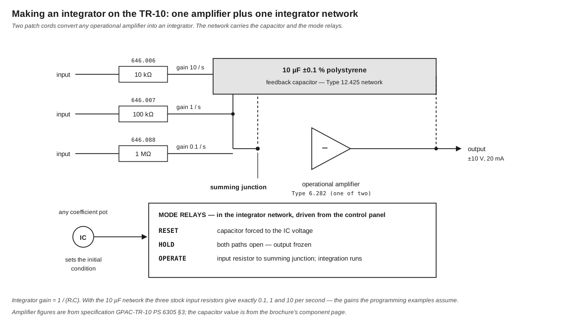
Figure 3 — An amplifier plus an integrator network. The three stock input resistor values give integrator gains of 0.1, 1 and 10 per second against the 10 µF capacitor. Diagram authored for this dive.
3.4.2 Integrator Gain
The gain of an integrator is 1/(R_i C). With the network’s 10 µF capacitor and the catalogued input resistors, the available gains are exact decades:
Table 4 — The gain of an integrator is 1/(R\i C). With the network's 10 µF capacitor and the catalogued input resistors, the available gains are exact decades
| Input resistor | Type | R_i C | Integrator gain |
|---|---|---|---|
| 1 kΩ | 646.005 | 10 ms | 100 per second |
| 10 kΩ | 646.006 | 100 ms | 10 per second |
| 100 kΩ | 646.007 | 1 s | 1 per second |
| 1 MΩ | 646.088 | 10 s | 0.1 per second |
This is not a coincidence of convenient values; it is why the capacitor is 10 µF. The gains of 1 and 10 are the ones the brochure’s worked programs actually use, and the factor-of-ten steps are what allow a scaled equation to be realised by choosing a resistor rather than by trimming a potentiometer.
3.4.3 The Two Type Numbers
The brochure gives the integrator network two different type numbers, and the distinction is real but is obscured by an apparent misprint.
Table 5 — 4.3 The Two Type Numbers
| Number | Where it appears | What it denotes |
|---|---|---|
| 12.263 | Standard Basic complement list (p. 12); the Standard Non-Linear Expanded complement (p. 13); the rep-op page describing what the rep-op network “replaces” | the real-time integrator network |
| 12.425 | The component specification heading (p. 8); the rep-op integrator network description (p. 7); the module’s own silkscreen, “INT NET 12.425”; the German dealer newsletter | the repetitive-operation integrator network |
| ”12.245” | The position-rule paragraph (p. 12) only | almost certainly a transposition of 12.425 |
The evidence for the transposition is strong. The brochure’s own component-specification page is headed 12.425, the photographed module face reads 12.425, and EAI’s German dealer newsletter of July 1965 independently refers to “network L2.425” — an OCR rendering of 12.425 — when describing the TR-10 integrator network. No source other than that single paragraph uses 12.245.
Vol 5 §3 covers what the rep-op network does differently.
3.5 Coefficient Potentiometers
3.5.1 Dual Coefficient Setting Potentiometer, Types 42.187 and 42.188
Table 6 — 5.1 Dual Coefficient Setting Potentiometer, Types 42.187 and 42.188
| Property | Value | Source |
|---|---|---|
| Pots per module | 2 | brochure |
| Maximum in attenuator row | 10 modules = 20 pots | brochure p. 12 |
| Type 42.187 | two ten-turn 5000 Ω carbon pots, adjusting knobs, push-button switch | brochure |
| Type 42.188 | two ten-turn 5000 Ω wire-wound pots, calibrated adjusting dial, push-button switch | brochure |
| Resolution | 0.025 % typical | spec §4.3 |
| Grounding | one pot bottom-end-grounded, one ungrounded, per module | brochure |
| Ungrounded proportion required | approximately one in two | spec §4.4 |
| Inputs | uncommitted | spec §4.5 |
| Patch panel | 5 in × 1½ in; brown (knob area), yellow (patching area) | brochure |
Two points of practical consequence.
Grounded and ungrounded. A grounded potentiometer divides a voltage against ground and produces k·e. An ungrounded one can be connected between two arbitrary nodes and is what allows a coefficient to be applied to a difference, or a pot to be floated in a feedback path. Specification §4.4’s requirement that roughly half be ungrounded is a statement about the range of problems the machine was meant to handle. The brochure notes that “a ground termination is located on the patch panel module so that ungrounded potentiometers may be conveniently grounded, if desired” — the flexible case is the default, and grounding is a patch.
The push-button. Each module carries a push-button switch that “connects reference to top of potentiometer and allows coefficient setting to be monitored by null meter”. This is what makes 0.025 % resolution usable: the operator sets the coefficient against the null meter, in circuit, without patching (Vol 2 §6.4).
3.5.2 Quad Coefficient Setting Potentiometer Group, Type 2.128
An assembly rather than a single module, and the reason the machine’s pot count reaches 24 rather than 20.
Table 7 — 5.2 Quad Coefficient Setting Potentiometer Group, Type 2.128
| Component | Type | Location |
|---|---|---|
| Quad Coefficient Setting Potentiometer Patching Module | 12.265 | non-linear row, position #20 only |
| Quad Coefficient Setting Potentiometer Assembly | 42.185 | control panel, position CP3 |
The group provides four additional potentiometers: “Four wire-wound, 5000 Ω ten-turn potentiometers are located on the mounting panel, each equipped with calibrated adjustment dials. They provide an indication of the coefficient setting and permit accurate resetting and recording of dial reading.” Two-hole terminations are provided on the patch panel for the four attenuators, and “the bottom ends of all four potentiometers are internally grounded”.
Twenty pots in the attenuator row plus these four is exactly the twenty-four of specification §1.4.
3.6 Multipliers
3.6.1 Multiplier, Type 7.045
Table 8 — 6.1 Multiplier, Type 7.045
| Property | Value | Source |
|---|---|---|
| Technique | quarter-square | brochure; spec §5.1 |
| Maximum in console | 9, positions #1–#18 | brochure p. 12 |
| Module width | full width (occupies an adjacent position pair) | brochure p. 12 |
| Function | produces −XY/10 from inputs +X, −X, +Y, −Y, with an external amplifier | brochure |
| Output polarity | reversible by interchanging +X, −X, +Y, −Y | brochure |
| Division | ”division of two variables may be readily performed” | brochure |
| Maximum static error | ≤ ±0.4 % of full scale (20 V full scale) | spec §5.2 |
| Phase shift, ±10 V DC by 20 V p-p at 1 kc | < 0.28° | spec §5.3 |
| Dynamic amplitude error, same conditions | ≤ ±0.25 % of full scale | spec §5.4 |
| Construction | completely solid state | brochure; spec §5.5 |
| Patch panel | 5 in × 1½ in; brown (in/out), black (ground), red (+ref), yellow (−ref) | brochure |
The divide-by-ten is not an artefact to be worked around; it is the scaling convention that keeps products inside the ±10 V range. Two variables each at full scale would produce 100 V without it. Because of it, a product of two full-scale quantities is itself full scale, and the factor of ten reappears in every scaled equation involving a product — visibly so in the Van der Pol program of Vol 4 §7.
The brochure adds a layout note worth recording: “Only the right half of the patch panel on the multiplier chassis is used for multiplier terminations. The left half provides reference and ground terminations for use as required for problem solution.”
3.7 Function Generators
3.7.1 Variable Diode Function Generator, Types 16.154 / 16.156 / 16.165
Three models, differing only in the input polarity range they accept. Used with two transistorised operational amplifiers, each represents an arbitrary function of one variable by straight-line segments.
Table 9 — 7.1 Variable Diode Function Generator, Types 16.154 / 16.156 / 16.165
| Type | Input range | Segments |
|---|---|---|
| 16.165 | ±10 V to +10 V (± input voltage) | 11 straight line segments |
| 16.156 | 0 to +10 V (+ input voltage) | 10 straight line segments |
| 16.154 | −10 to 0 V (− input voltage) | 10 straight line segments |
Table 10 — 7.1 Variable Diode Function Generator, Types 16.154 / 16.156 / 16.165
| Property | Value |
|---|---|
| Output voltage range | ±10 V DC, all models |
| Adjustment | by screwdriver from the side of the DFG chassis when mounted in Service Shelf Type 51.039 |
| Set-up aid | Set-Up Attenuator Unit Type 42.243 |
| Position | any even-numbered position except #20 |
| Patch panel | 5 in × ¾ in; brown |
Note — The brochure names the middle model 16.156 on its component page and 16.155 in its position-rule paragraph. Only one of those can be right and the held sources do not resolve which. A surviving module’s silkscreen would settle it.
3.7.2 X² Diode Function Generator, Type 16.101
A dual fixed diode function generator. One dual chassis, with one or two external amplifiers, performs:
- X² output for an X input of one polarity (one amplifier);
- (X₁)² and (X₂)² where X₁ and X₂ are unipolar and of opposite sign (two amplifiers);
- X² for an input X varying both plus and minus in sign (two amplifiers);
- square root, by placing the X² DFG in the feedback loop of an operational amplifier.
Table 11 — 7.2 X² Diode Function Generator, Type 16.101
| Property | Value | Source |
|---|---|---|
| Input | ±10 V | brochure |
| Output | ±10 V | brochure |
| Segments per quadrant | at least seven | spec §6.4 |
| Maximum static error | ≤ ±0.4 % of full scale; typical ≤ ±0.2 % | spec §6.5 |
| Position | any even-numbered position except #20 | brochure p. 12 |
| Patch panel | 5 in × ¾ in; brown | brochure |
The square-root trick is the general principle of analog non-linear computing and is worth stating explicitly: putting a function generator in the feedback path of an amplifier produces the inverse function. The amplifier drives its output to whatever value makes the generator’s output cancel the input, and that value is the inverse. No separate square-root hardware is required.
Specification §6.2 lists the same four operations and adds that the machine “shall be capable of” them — the specification and the brochure agree closely here, which is not true everywhere.
3.7.3 Log Diode Function Generator, Types 16.126 and 16.133
Table 12 — 7.3 Log Diode Function Generator, Types 16.126 and 16.133
| Type | Output, with one external amplifier |
|---|---|
| 16.126 | 5 log₁₀(10X) for an X input |
| 16.133 | 2.5 log₁₀(10X) for an X input |
One dual chassis of either type performs log X for an input of one polarity (one external amplifier); log₁₀X₁ and log₁₀X₂ for unipolar inputs of opposite sign (one amplifier per channel); and — by the same feedback principle as §7.2 — an exponential output by placing the log DFG in the feedback loop of an external amplifier.
Table 13 — 7.3 Log Diode Function Generator, Types 16.126 and 16.133
| Property | Value |
|---|---|
| Input range | ±10 V DC |
| Output range | ±10 V DC |
| Position | any even-numbered position except #20 |
| Patch panel | 5 in × ¾ in; brown |
3.8 Switching and Decision Elements
3.8.1 Comparator, Type 6.143
Table 14 — 8.1 Comparator, Type 6.143
| Property | Value | Source |
|---|---|---|
| Function | compares a variable input voltage to an arbitrary bias voltage and causes a switching operation | brochure; spec §7.1 |
| Construction | three-stage transistor amplifier and a high-speed double-pole double-throw relay | brochure |
| Relays required | at least one DPDT | spec §7.2 |
| Differential amplifier | furnished as part of the comparator | spec §7.3 |
| Input range | ±10 V | spec §7.4 |
| Switching time | ≤ 10 ms | spec §7.5 |
| Sensitivity | ≤ 3 mV | spec §7.6 |
| Contact rating | at least 2 A at 30 V, non-inductive | spec §7.7 |
| Position | #18 only | brochure p. 12 |
| Patch panel | 5 in × ¾ in; green (inputs), red (relay contacts) | brochure |
The brochure states the logic: “When the algebraic sum of input variable and bias voltage is positive, the relay will assume one position and, when this sum is negative, it will assume the other.”
The comparator is what lets an analog machine represent a discontinuity — a limit stop, a switching control law, a contact opening. It is also the machine’s one concession to decision-making, and its 10 ms switching time places a hard floor under how fast a discontinuous problem can be run. In repetitive operation at 20 ms per solution (Vol 5), a 10 ms relay is half the compute interval; a comparator-driven problem cannot be run at the fastest repetition rates.
3.8.2 Dual Function Switch Group, Type 2.127
Table 15 — 8.2 Dual Function Switch Group, Type 2.127
| Component | Type | Location |
|---|---|---|
| Function Switch Patching Module | 12.264 | non-linear row, position #19 only |
| Dual Function Switch Mounting Panel | 20.366 | control panel, position CP2 |
Two independent single-pole, double-throw, centre-off switches for manual switching operations, with two ground terminations provided on the patch panel for general use.
Table 16 — 8.2 Dual Function Switch Group, Type 2.127
| Property | Value | Source |
|---|---|---|
| Switch type | SPDT, centre off | brochure; spec §8.1 |
| Contact rating | 120 V, 1.0 A resistive | brochure; spec §8.2 |
| Patch panel | 5 in × ¾ in; red (switch contacts), black (ground) | brochure |
The purpose, in the brochure’s words, is to “provide for manually interchanging components without reprogramming or repatching” — changing a problem parameter or swapping an element in or out by throwing a switch instead of moving cords.
3.9 Reference, Tie Points and Accessories
3.9.1 Reference Panel, Type 12.266
Makes ±10 V reference available at the patch panel. The brochure notes an important dependency: “A similar panel is also included as a part of Multiplier, Type 7.045, and used for the same purpose. Computers that do not use the Multiplier, Type 7.045, will use the Reference Panel, Type 12.266, for obtaining the necessary reference terminations.”
Table 17 — 9.1 Reference Panel, Type 12.266
| Property | Value |
|---|---|
| Output | ±10 V |
| Supply capacity | 50 mA (spec §9.1) |
| Parallel terminations required | ≥ 3 positive, ≥ 3 negative (spec §9.2) |
| Position | any even-numbered position except #20 |
| Patch panel | 5 in × ¾ in; red (+ref), yellow (−ref), black (ground) |
3.9.2 Dual Tie Point Panel, Type 12.267
Two four-hole tie points for multiple interconnections of patch cords, or for increasing the number of output terminations of a computing component. May be positioned anywhere in the non-linear row — the only module with no positional restriction.
Patch panel: 5 in × ¾ in; white.
3.9.3 Overload Alarm, Type 13.012
Audible warning when any operational amplifier overloads; tone adjustable; fully transistorised; mounts at the rear of the computer adjacent to the reference regulator. Housed in a standard TR-10 component chassis, 5 in × 1½ in, colour code yellow. Part of the Standard Basic complement.
3.9.4 Set-Up Attenuator Unit, Type 42.243
A small, separate rotary-switched unit — not a console module — for setting up the variable DFG. “When plugged into an operational amplifier and with reference voltage patched to its input it provides a precision voltage divider for the convenient setting of VARIABLE DFG breakpoint voltages. Amplifier output voltage can be stepped in increments of 1 volt by rotary switch on front of Attenuator Unit. Polarity of voltage output determined by polarity of reference voltage patched to input.”
3.9.5 Service Shelf, Type 51.039
Facilitates maintenance of any plug-in computing component under normal operating conditions — see Vol 2 §3.3. Also the mounting used when adjusting a variable DFG’s breakpoints.
3.10 Patching Accessories
These are the consumables of analog programming, and they carry type numbers like everything else.
3.10.1 Feedback Resistors
Wire-wound, ±0.1 %, supplied in blue moulded plugs, designed for patching between the summing junction and output terminations of any operational amplifier.
Table 18 — 10.1 Feedback Resistors
| Type | Value | Code |
|---|---|---|
| 646.010 | 10,000 Ω | Red Dot |
| 646.021 | 100,000 Ω | Yellow Dot |
The brochure notes that feedback resistors may be paralleled “by plugging one plug on top of another plug” — specification §11.1.3 requires exactly this. Paralleling two 100 kΩ feedback resistors halves the feedback resistance and so halves every gain through that amplifier at once.
Note — Specification §11.1.1 requires feedback resistors of 100 kΩ only. The brochure catalogues two values. The shipped product exceeded the specification here; see Vol 6.
3.10.2 Input Resistors
Epoxy-encapsulated, wire-wound, ±0.1 %. “Male end plugs into amplifier summing junction terminations, female end accepts patch cord plug” — the resistor is physically in line with the patch cord, not a separate component on a board.
Table 19 — 10.2 Input Resistors
| Type | Value | Colour code |
|---|---|---|
| 646.005 | 1,000 Ω | Red Band |
| 646.006 | 10,000 Ω | Orange Band |
| 646.007 | 100,000 Ω | Yellow Band |
| 646.088 | 1 megohm | Green Band |
Against a 100 kΩ feedback resistor these give summer gains of 100, 10, 1 and 0.1. Against a 10 kΩ feedback resistor the 1 kΩ and 10 kΩ inputs give 10 and 1. The decade structure of the machine’s gains comes entirely from this small set of parts.
Specification §11.2.1 requires only 10 kΩ and 100 kΩ input resistors — again, fewer than shipped.
3.10.3 Resistor Set, Type 5.134
Table 20 — 10.3 Resistor Set, Type 5.134
| Quantity | Type | Description |
|---|---|---|
| 15 | 646.006 | 10 kΩ input |
| 10 | 646.007 | 100 kΩ input |
| 10 | 646.010 | 10 kΩ feedback |
3.10.4 Diode Unit, Type 614.051
A white-banded, epoxy-encapsulated silicon diode “for limiting the output of computing components or generating non-linear effects”.
Table 21 — 10.4 Diode Unit, Type 614.051
| Property | Requirement | Source |
|---|---|---|
| Maximum inverse voltage | at least 25 V | spec §11.3.2 |
| Inverse current | 0.025 µA at 10 V | spec §11.3.3 |
| Minimum forward current | at least 3 mA at 1 V | spec §11.3.3 |
Note — Specification §11.3.3 reads “Maximum inverse current shall be at least .025 microamperes at 10 volts.” A maximum that “shall be at least” a value is self-contradictory as drafted; the intent is evidently a leakage ceiling of 0.025 µA. Recorded here as it stands.
The diode plug matters out of proportion to its size. A diode patched across an amplifier’s feedback resistor limits the output; a pair with opposite polarity and different bias voltages creates a dead zone; a diode in series with an input creates a half-wave term. These are how the machine represents backlash, saturation, limit stops and rectification without a function generator.
3.10.5 Multiple Block, Type 542.605
A six-hole, off-the-patch-panel tie point for interconnecting patch cords or increasing the number of output holes of computing components. Specification §11.4.1 describes the same part.
3.10.6 Patch Cord Set, Type 5.133
Colour-coded by length, which is a small but real ergonomic decision: the operator picks a cord by the distance it has to span, not by trial.
Table 22 — 10.6 Patch Cord Set, Type 5.133
| Quantity | Type | Length | Colour |
|---|---|---|---|
| 10 | 510.043-0 | 6 in | Black |
| 15 | 510.043-1 | 12 in | Brown |
| 10 | 510.043-2 | 18 in | Orange |
| 5 | 510.043-3 | 30 in | Blue |
Specification §11.5.2 requires that patch cords “be color coded as to their length”, and §11.5.3 that “their plugs shall fit all jacks used in the computer”.
3.11 The Two Standard Configurations
EAI sold the TR-10 in named complements. These are the two the brochure documents.
3.11.1 Standard Basic TR-10
“Provides an economical desk-top analog computer with all of the quality engineered features of the expanded TR-10 Computer… and expansion capabilities are built right in.” Capable, per the brochure, of “solving up to two second-order differential equations plus associated linear algebraic operations”.
Table 23 — 11.1 Standard Basic TR-10
| Qty | Component |
|---|---|
| 1 | Pre-wired Console |
| 1 | Reference System |
| 1 | Power Supply |
| 1 | Overload Alarm |
| 5 | Dual Coefficient Setting Potentiometers (Type 42.187) |
| 5 | Dual Transistorized Operational Amplifiers |
| 2 | Dual Integrator Networks (Type 12.263) |
| 1 | Dual Tie Point Panel |
| 1 | Reference Panel |
| 1 | Patch Cord Set |
| 1 | Multiple Block |
| 1 | Resistor Set |
| 1 | Diode Unit |
| 1 | Service Shelf |
Ten amplifiers, ten potentiometers, four integrators.
3.11.2 Standard Non-Linear Expanded TR-10
Designated TR-10-3 in the brochure’s table. “Experience has shown that the complement of computing components provided in the Standard Non-Linear Expanded TR-10 will satisfy the computing requirements of typical engineering design problems.”
Table 24 — 11.2 Standard Non-Linear Expanded TR-10
| Qty | Component |
|---|---|
| 1 | Pre-wired Console |
| 1 | Power Supply |
| 1 | Reference System |
| 1 | Overload Alarm |
| 10 | Dual Coefficient Pots (Type 42.187) |
| 1 | Quad Coefficient Pots |
| 10 | Dual Operational Amplifiers |
| 4 | Dual Integrator Networks (Type 12.263) |
| 2 | Multiplier (Type 7.045) |
| 1 | VARIABLE DFG (Type 16.165) |
| 1 | X² DFG (Type 16.101) |
| 1 | Set-Up Attenuator Unit |
| 1 | Comparator |
| 3 | Dual Tie Point Panel |
| 1 | Dual Function Switch Group |
| 1 | Service Shelf |
| 3 | Patch Cord Set |
| 1 | Multiple Block |
| 2 | Resistor Set |
| 1 | Diode Unit |
| 1 | High Speed Rep Op Group (optional) |
Twenty amplifiers, twenty-four potentiometers, eight integrators, two multipliers, two function generators, one comparator. This is the fully expanded machine to which the 95 lb and under-50 W figures of Vol 1 refer.
3.11.3 Slaving
Beyond the expanded single console, the brochure offers one more step: “If your problem becomes too large for a single expanded TR-10 then you slave two TR-10’s together… With the TR-10 SLAVE feature you have complete control of your problem solution… from either computer. TR-10 Computers are easily SLAVED… or disconnected to permit the solution of two individual problems simultaneously.” Specification §11.6.5 requires the slave system to “allow control of two or more computers in either real time or repetitive operation mode”.
3.12 What Comes Next
Vol 4 takes this catalogue and uses it: an ordinary differential equation is scaled, translated into amplifiers, pots and networks, and checked against the brochure’s own worked examples. Vol 5 returns to the integrator networks for time scaling and the high-speed repetitive operation accessory. Vol 6 sets every figure in this volume against its source and lists the divergences noted here in §4.3, §7.1, §10.1, §10.2 and §10.4.
Comments (0)