Aeon Dynamic Simulator · Volume 4
Aeon Dynamic Simulator — Volume 4 — Inside the case
The board stack, the semiconductor complement read device by device off two photographs, the trimmer banks and the letter-coded resistor system — and the precise point at which the absence of a schematic stops the analysis
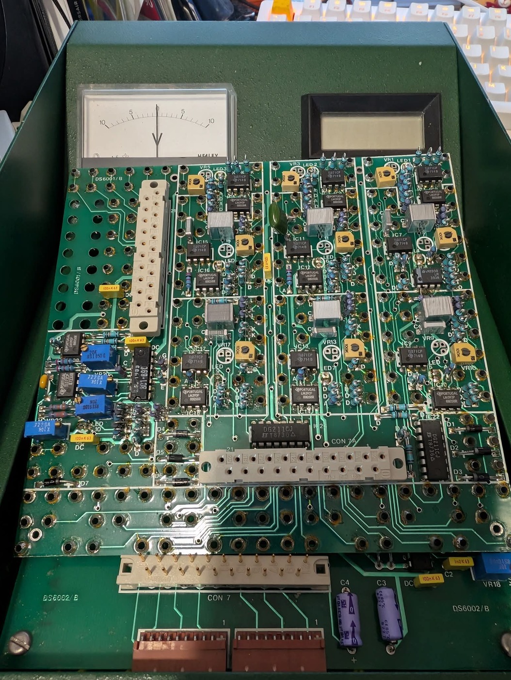
Figure 1 — The machine opened. The board beneath the patch field is organised as repeated vertical groups, one per computing element, each with its own trimmer, indicator LED and pair of integrated circuits. Crop of a locally held photograph.
4.1 About this Volume
This volume reports what the two interior photographs show: the boards, their designations, the semiconductor devices on them with their markings quoted verbatim, the trimmers, the test points and the resistor coding system.
It also marks a boundary, and does so early because it governs everything that follows. No schematic for this machine is held, and a circuit cannot be recovered from photographs of populated boards. Traces disappear under components, both sides of no board are visible, and no photograph shows the underside of the main board at all. This volume can therefore say what devices are present, in what quantity, and in what arrangement relative to one another. It cannot walk a signal from a jack to an amplifier output, and it does not attempt to. Every functional claim below is labelled as the inference it is.
Cross-references: Vol 1 for dating from these devices; Vol 3 for the elements these boards implement; Vol 6 for what the switching devices imply about the modes.
4.2 What the Photographs Show, and in What Order
The two interior photographs are two different states of disassembly, not two angles on one state.
- Photograph 2 shows the patch board displaced, exposing the component side of a board organised into repeated vertical groups — one group per computing element.
- Photograph 3 shows the jack board hinged up and leaning back on its harness, exposing a board whose component side is entirely different in character: rows of axial resistors, a bank of identical trimmers, and a silkscreened legend table.
In both photographs the same strip is visible along the bottom edge — the connector CON 7, two brown connectors, the electrolytics C3 and C4, and the designation DS6002/B silkscreened at both left and right. That strip anchors the two views to each other.
4.2.1 The Board Stack, and an Honest Ambiguity
Two board designations are legible:
Table 1 — Two board designations are legible
| Designation | Where it appears | What it carries |
|---|---|---|
DS6001/B | on the jack board, twice | the patch sockets; the printed overlay is on its outer face |
DS6002/B | on a board beneath, twice | visible along the bottom edge in both interior photographs |
What cannot be resolved is how many boards there are. The repeated amplifier groups of photograph 2 and the resistor rows and trimmer bank of photograph 3 are different component layouts, yet the DS6002/B silkscreen appears along the bottom edge of the visible board in both. Either the machine is a two-board stack photographed at two different lift angles, with the upper region of DS6002/B obscured in one view and exposed in the other, or there is a third, intermediate board carrying the amplifier groups whose own designation is never legible.
Three photographs do not settle it, and it is recorded here as unresolved rather than decided by preference. What is certain is that the jack board is a separate assembly from the computing electronics, connected by a harness, and that at least one further board lies beneath it.
Connectors legible across the two photographs are CON6, CON 7 and CON 7A, together with several white and brown multi-way headers; one carries the numerals 1 and 21, indicating a 21-way part.
4.3 The Semiconductor Complement
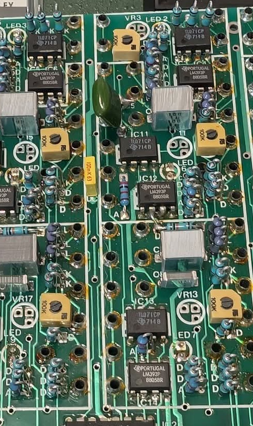
Figure 2 — A computing group. The pairing of one TL071CP with one LM393P, repeated down the board with a trimmer and an LED beside each, is the structural signature of this machine’s electronics. Crop of a locally held photograph.
Markings are transcribed exactly as they read in the photographs. Where a marking is ambiguous at photographic resolution, that is stated.
Table 2 — The Semiconductor Complement
| Marking as read | Device class | Quantity observed | Function in this machine |
|---|---|---|---|
TL071CP with 714B / 714D beneath, and the Texas Instruments logo | single JFET-input operational amplifier | many — at least one per computing group | the computing amplifier (inference) |
PORTUGAL / LM393P / 8805BR with the TI logo | dual differential comparator | one per computing group | overload detection driving the panel LEDs (inference) |
LM / 393N with M8930 above | dual differential comparator | at least one | as above |
PORTUGAL / TL072CP / 8723XA | dual JFET-input operational amplifier | several, on the lower board | buffering, reference or metering (inference) |
DG211CJ with T8730 △ and T8736 △ | quad SPST analogue switch | two observed | mode switching (inference) |
14-pin DIP reading LSL 1409 / 3C1-69C | not identified | one | unknown |
4.3.1 What Each Device Class Implies
The TL071CP as the computing amplifier. The TL071 is a JFET-input operational amplifier, and JFET inputs are exactly what an integrator wants: input bias current is what makes an integrator drift when it should be holding, and a bipolar-input amplifier drifts faster. Finding one TL071CP in each repeated group, alongside the film capacitor that the panel legend identifies as the integrating capacitor, is consistent with the TL071CP being the amplifier drawn as a triangle on the panel.
This is an inference from position and device type. The panel names no device, and no trace was followed from a jack to a pin.
The LM393P as the overload detector. The LM393 is a dual comparator — a device for deciding whether one voltage has passed another, which is not something a computing path needs. Its presence once per computing group, beside an amplifier and an LED, is the layout of an overload indicator: compare the amplifier’s output against a threshold near the supply rails, and light a lamp when it is exceeded. A dual comparator suits this exactly, one half for each polarity. Vol 3 reads the red discs drawn inside every amplifier triangle on the panel as overload lamps, and this is the hardware that supports that reading.
The DG211CJ as the mode switch. The DG211 is a quad SPST analogue switch — four independently controlled solid-state contacts in one package. On an analogue computer the job that needs exactly this is mode control: shorting or steering each integrating capacitor on RESET, isolating it on HOLD, releasing it on RUN. Two such packages give eight switched paths.
That the machine switches modes electronically rather than with relays is itself a statement of date. A 1960s machine of this class used a relay with several contact sets; by the late 1980s a pair of CMOS switch packages did the same job silently, faster, and without contact bounce. Vol 6 develops the consequences.
The TL072CP on the lower board. A dual version of the same amplifier family, in a region of the board given over to resistor networks rather than to the repeated computing groups. Reference generation, metering and the interface column are the plausible duties. This is the least constrained inference in the volume and is held loosely.
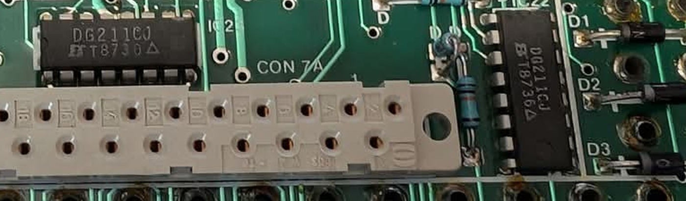
Figure 3 — The two DG211CJ quad analogue switches, date-coded T8730 and T8736. Crop of a locally held photograph.
4.3.2 The Unidentified Device
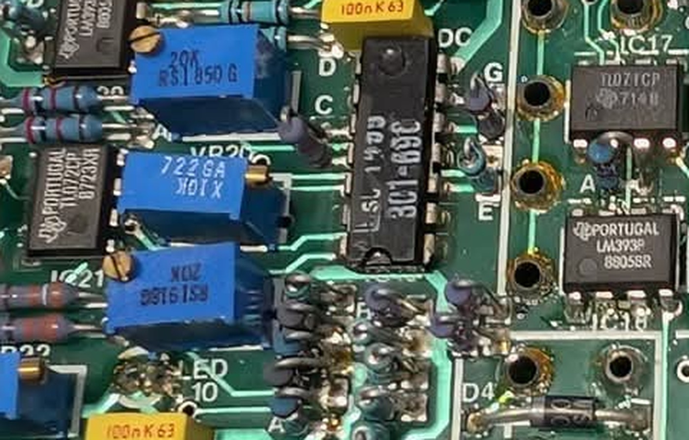
Figure 4 — The lower-left region, carrying the machine’s multiturn trimmers VR20, VR21 and VR22, and the 14-pin device that could not be identified. Crop of a locally held photograph.
One 14-pin plastic DIP at the lower left of the computing board carries markings that read, with the device rotated, as LSL 1409 and 3C1-69C. No manufacturer logo is legible. Neither string corresponds to a device identified here, and no function is assigned to it. Its position — among the multiturn trimmers and close to the electrolytics and the reference test points — is suggestive of the reference or supply section, but that is proximity, not evidence.
It is recorded as unidentified. Vol 7 lists it among the questions a schematic or a clearer photograph would answer.
4.3.3 On Counting the Amplifiers
A precise device count is not possible from these photographs. Designators as high as IC22 are legible, and LED 10 appears on the silkscreen, but parts of every board are obscured by the displaced patch board, by the harness, or by the angle of view. The panel legend gives the authoritative count of computing elements — nine amplifier-based elements plus the multiplier, as Vol 3 sets out. The number of amplifier packages inside will be larger than nine, because reference generation, metering and the interface column all need amplifiers of their own, and no useful figure can be given for how much larger.
4.4 The Trimmers
Three distinct populations of adjustable component are visible, and they are worth separating because they imply three different kinds of adjustment.
Table 3 — The Trimmers
| Type | Marking | Designators seen | Location | Reading |
|---|---|---|---|---|
| Yellow single-turn cermet | 100K | VR1, VR3, VR5, VR9, VR10, VR13, VR17 | one per computing group | per-element adjustment — offset null or gain trim |
| Blue multiturn | 20K (RS1 850 G), 10K (722GA X10K), and a further 20K | VR20, VR21, VR22 | lower left, near the electrolytics | reference or supply setting |
| Blue multiturn, in a bank | 100K | VR1–VR16 | lower board, two columns of eight | see below |
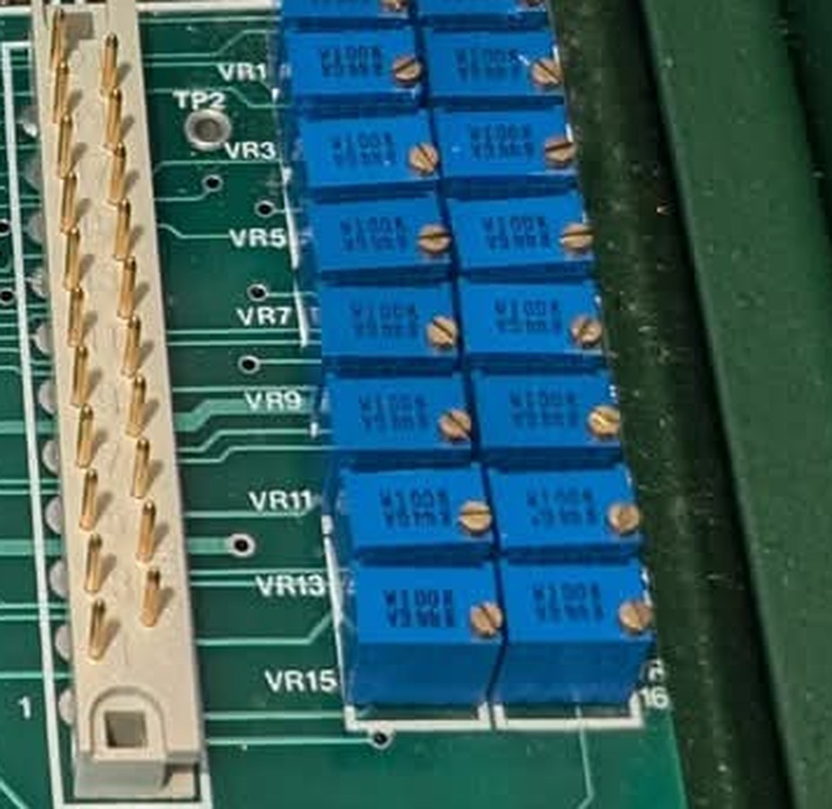
Figure 5 — The trimmer bank on the lower board: sixteen identical 100 kΩ multiturn trimmers, designated VR1 through VR16. Crop of a locally held photograph.
The bank of sixteen is the most informative of the three. Sixteen identical multiturn trimmers in a regular array, on a board separate from the computing groups, is the signature of a systematic per-channel calibration rather than of a one-off adjustment. Multiturn parts are chosen where a setting must be made precisely and must stay put.
What they trim cannot be established. Sixteen is not an obvious multiple of any element count on this machine — there are nine amplifier elements, six pots, six diodes and six reference strips — so the bank does not map cleanly onto any one class of element. Note also that the designators VR1, VR3, VR5 and so on recur on both the computing board and this bank, which means the two boards number their components independently and a designator alone does not identify a part on this machine.
4.5 The Letter-Coded Resistor System
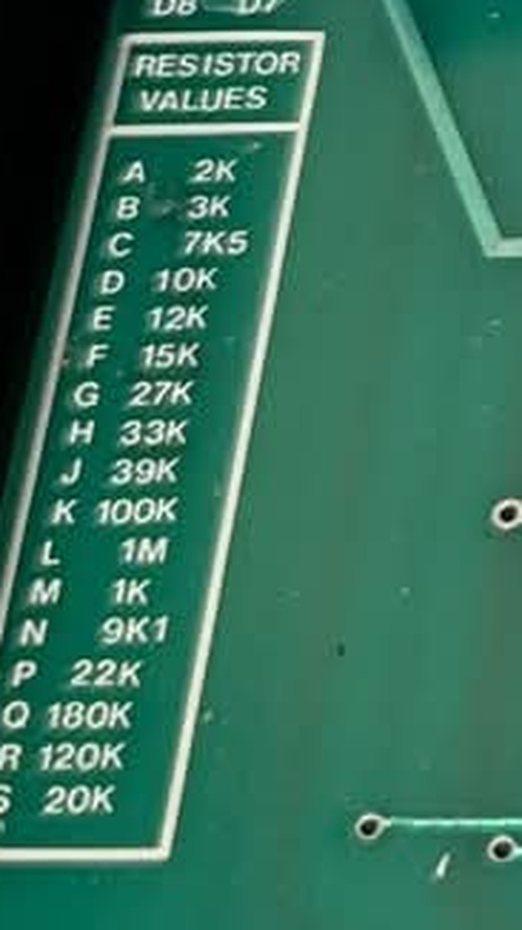
Figure 6 — The RESISTOR VALUES legend, silkscreened on the lower board. Crop of a locally held photograph.
The lower board carries a silkscreened table headed RESISTOR VALUES, mapping single letters to resistances. Transcribed in full, in the order printed:
Table 4 — The lower board carries a silkscreened table headed RESISTOR VALUES, mapping single letters to resistances. Transcribed in full, in the order printed
| Letter | Value | Letter | Value | |
|---|---|---|---|---|
| A | 2 kΩ | L | 1 MΩ | |
| B | 3 kΩ | M | 1 kΩ | |
| C | 7·5 kΩ | N | 9·1 kΩ | |
| D | 10 kΩ | P | 22 kΩ | |
| E | 12 kΩ | Q | 180 kΩ | |
| F | 15 kΩ | R | 120 kΩ | |
| G | 27 kΩ | S | 20 kΩ | |
| H | 33 kΩ | |||
| J | 39 kΩ | |||
| K | 100 kΩ |
Seventeen values. The letters I and O are omitted, which is standard engineering practice to avoid confusion with the numerals 1 and 0, and the sequence is otherwise unbroken from A to S.
Instead of printing a resistance beside each resistor position, the board silkscreens a letter. Letters K, L, D, A, N, S and M are directly legible beside components in the photographs of both boards. The values they stand for are the ones the panel legend already advertises — K is the 100 kΩ of the summers, L the 1 MΩ of the integrator inputs, D the 10 kΩ — which ties the interior coding to the exterior legend and confirms the two describe the same machine.
The scheme is a production convenience: a single legend table serves the whole board, silkscreen area beside each component is saved, and an assembler or a repairer reads the letter and consults the table. It is also, incidentally, another instance of this machine’s governing habit — putting the documentation on the hardware. Vol 2 observed that the patch field is a schematic rather than a set of labels; this is the same instinct applied to the inside of the machine. A board that carries its own bill of materials can be repaired without the paperwork, which is precisely the situation this series finds itself in.
A caution: the table gives nominal values only. It states no tolerance and no power rating, and it cannot be used to determine the accuracy of any computing path.
4.6 Test Points, Power and the Integrating Capacitors
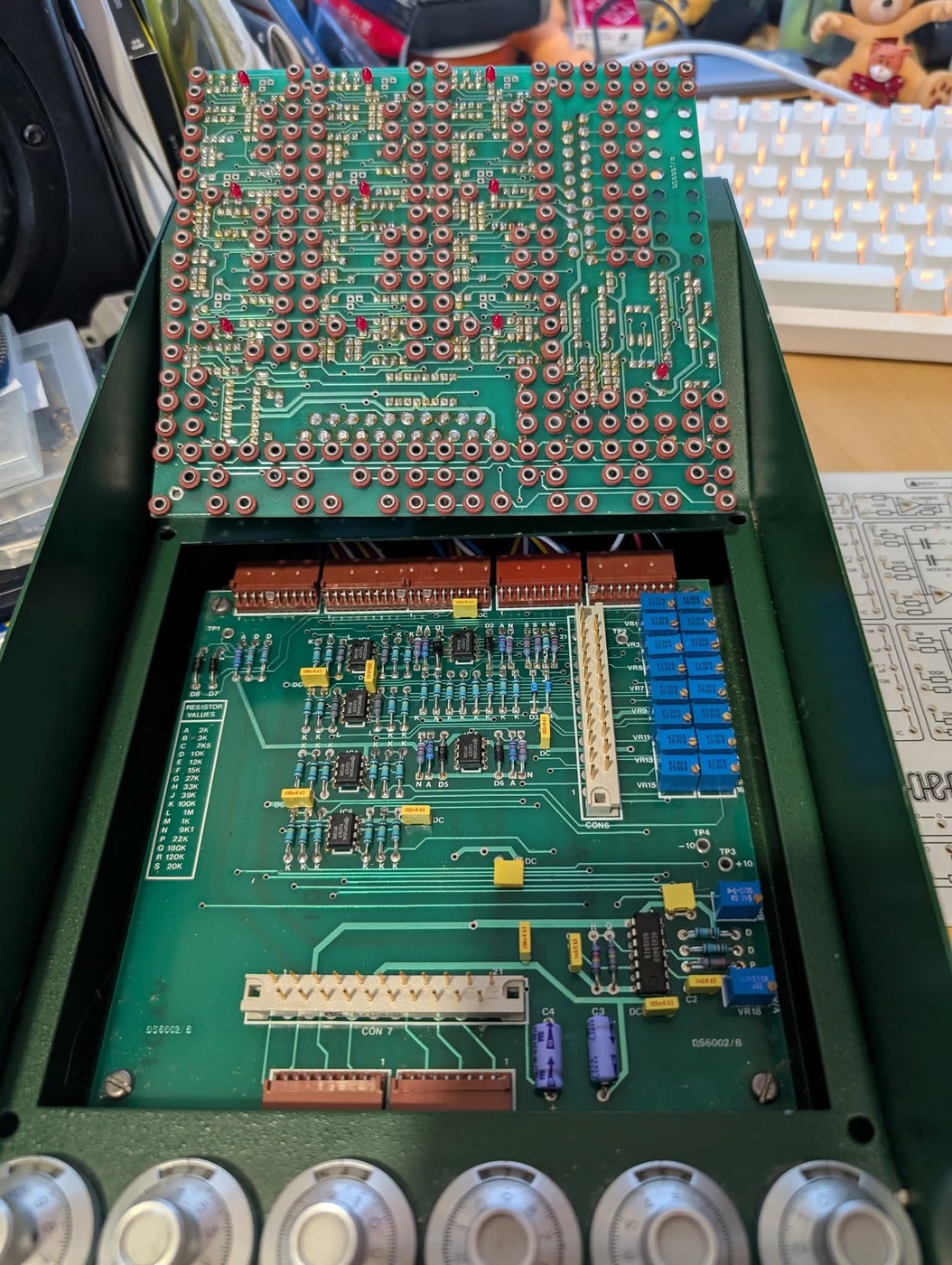
Figure 7 — The lower board. Crop of a locally held photograph.
Test points. Four are silkscreened: TP1, TP2, TP3 marked +10, and TP4 marked −10. The labelling of two of them with the reference voltages is significant out of proportion to its size — it confirms the ±10 V reference directly in the hardware, independently of the panel legend, and it identifies where any calibration of the machine would have to begin. Vol 6 builds a reconstructed calibration sequence around them.
Power. No mains transformer, mains inlet, fuse holder or power switch appears in any of the three photographs. The enclosure’s lower portion is not photographed. Whether the machine runs from an internal mains supply or an external low-voltage supply cannot be determined, and no supply-rail voltage is stated anywhere. Two electrolytic capacitors, C3 and C4, sit at the bottom edge of the board with a pair of polarity arrows visible on their sleeves, consistent with a split supply — but consistency is not evidence, and the rails are unknown.
The integrating capacitors. Each computing group carries one or two rectangular film capacitors in a light-coloured case, of the physical size that 1 µF and 0·1 µF parts take in that dielectric. The panel legend states those two values as the integrator feedback options, and these are the parts in the position to be them. No value or tolerance is legible on any of them in the photographs.
Passive decoupling. Yellow box capacitors marked 100nK63 — 100 nF, ±10 %, 63 V — are distributed across both boards in the pattern of supply decoupling, with at least one 1n0K63 also visible.
4.7 Where the Analysis Stops
It is worth stating explicitly what a schematic would settle, so that the limits of this volume are not mistaken for limits of the machine.
- The amplifier circuit. Whether each computing amplifier is a bare TL071CP or a composite with additional gain or output stages.
- How the modes are actually implemented. Which DG211 contact does what, whether HOLD isolates the capacitor or the input, and what the RESET path’s time constant is.
- How the initial condition is applied on integrators 1 and 2, and what, if anything, happens at the corresponding point on integrators 3 to 6 — the question Vol 3 leaves open.
- What the trimmers trim. Whether the per-group yellow trimmer is an offset null or a gain trim, and what the bank of sixteen calibrates.
- The reference circuit, its stability, and which device generates it.
- The interface column, and in particular where the conditioning lives that allows a ±10 V machine to feed a host expecting a much smaller range.
- The supply rails and their source.
- The identity and purpose of the 14-pin device at the lower left.
- Every performance figure — bandwidth, drift, offset, accuracy — none of which is recoverable from photographs under any circumstances.
Until such a document is produced, statements about any of the above, wherever they appear, should be treated as unsourced.
4.8 What Comes Next
Vol 5 leaves the hardware and turns the printed component values into the machine’s arithmetic: the ±10 V machine unit, the gain matrix the integrator inputs and feedback options generate, amplitude and time scaling, and a second-order problem patched onto the elements catalogued in Vol 3. Vol 6 returns to the mode lever and the readout, and builds a calibration sequence around the +10 and −10 test points identified above.
Comments (0)